Our goal is to train first-class employees, manufacture first-class products, build first-class enterprises, and make contributions to the development of the electronics industry.
Current Position: Home - news information
2018-11-22
Angie Brown
While gold plating is frequently used for printed circuits boards (PCBs), selecting the most useful gold PCB surface finish can be somewhat more of a mystery. Understanding the different compositions and practical uses of gold finishes such as ENIG, ENEPIG, and gold fingers can help you find the right finish to match your circuit board needs.
When you buy a gold product such as jewelry, the gold is measured by Karat (K). Karat is the unit used to measure the purity. The higher the “K” numbers, the purer the gold. 24K is the highest purity, 100% gold; high in bright yellow color. 22K and 18K are more commonly referred to when referring to jewelry as it is lesser in cost and higher in density. 24K gold is much softer and less likely to be used in wearable products. 22K gold is commonly used in fine jewelry as it is still yellow in color and shines well, it contains 91.67% gold with a remanding balance of 8.33% being silver, zinc, nickel, or other metals. 18K gold is 75% gold and 25% other metal such as copper or silver to add density to the product and is less expensive.
For all gold applications pertaining to PCBs, the purity is 99.9% pure gold making this surface finish, for what is actually a waste product at assembly, a pricey way to go. There are a lot of types of gold finishes applied to printed circuit boards, some remain part of the finished assembly while SMT devises and through-holes are used to protect the underlying finish and electroless nickel plating for the assembly process.
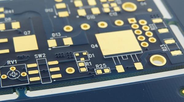
The most popular surface finish used by designers is a soft gold. Processed at 1-3 micro-inches, it is somewhat self-limiting and easily managed. Electroless nickel immersion gold (ENIG) as a surface finish has good oxidation resistance and is extremely flat when applied which eases processing challenges in assembly.

Keeping in mind that gold is a waste product, recently, we have seen design engineers increase their requests to add more gold. 4-8 micro inches for an example, adding this much gold requires added cost, added lead time, and adjusted standard processing during production. This limits the product that can move while these special orders process. So why increase the amount of gold? It can only be suspected that the areas required for rework processing the added gold may assist in preservation.
Per IPC-4552, the demand to increase the gold deposit may compromise the underlying nickel, the sole purpose is to protect the nickel, creating processing challenges for CMs.
Similar to ENIG, electroless nickel electroless palladium immersion gold (ENEPIG) only adds palladium to the alloy. When ENIG was first introduced, it had its own issues. Two to mention are non-wetting and black pad. It was thought that adding palladium to underlying nickel to protect and help with wetting would limit the issue.
The ENEPIG finish did not take off as expected. It added cost for the very expensive palladium coupled with a separate processing line, and soured manufacturing as well as the designers and buyers. This finish increased processing times and prices were increased 35-60% depending on the volume. Along with added cost, lead times are extended. Although the process is alive and well, typically it only runs once a month or when the line will be full.
This finish has some advantages for wire bonding and shelf life but it comes at a cost.

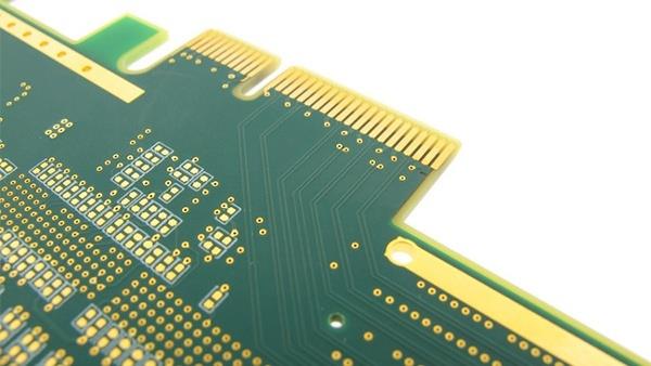
PCB Manufactured with Gold Fingers
Often a PCB is used in combination with a membrane switch where the underlying gold must withstand many actuation forces of a keypad. The gold plating on tabs of a keypad is usually defined by the engineer at 200-300 micro inches. Hard gold is meant to survive many actuation forces or insertion and removal up to 1,000 actuations or more.
To better understand the longevity, think of your keyboard or calculator. Each depression to make a contact must hold up to long usage. This type of gold plating is electroplated or electrolytic plated by using an electrical charge as opposed to a purely chemical reaction. Thickness may be controlled by varying the plating cycle time. Thickness is usually between .000015”-.000050” standard processing.
Flash electrolytic is a thin coating of hard gold. Unlike thicker hard gold coatings, flash gold remains solderable for SMT assembly because its coating thickness is approximately 10% as thick as hard tab gold. Like ENIG, its thickness range is limited – typically .0000015”-.000003” thick.
Be sure to ask your supplier questions specific to your application. It is also recommended to discuss requirements early in the design stages to build for the highest reliability and determine the best processes.